Third-author research / Published 2026
Numerical Investigation of Short-Channel Effects and RF Performance in Top-Gate In2O3 Thin-Film Transistors
A third-author contribution to a two-dimensional TCAD study of short-channel and RF scaling in top-gate In2O3 thin-film transistors.
Academic poster
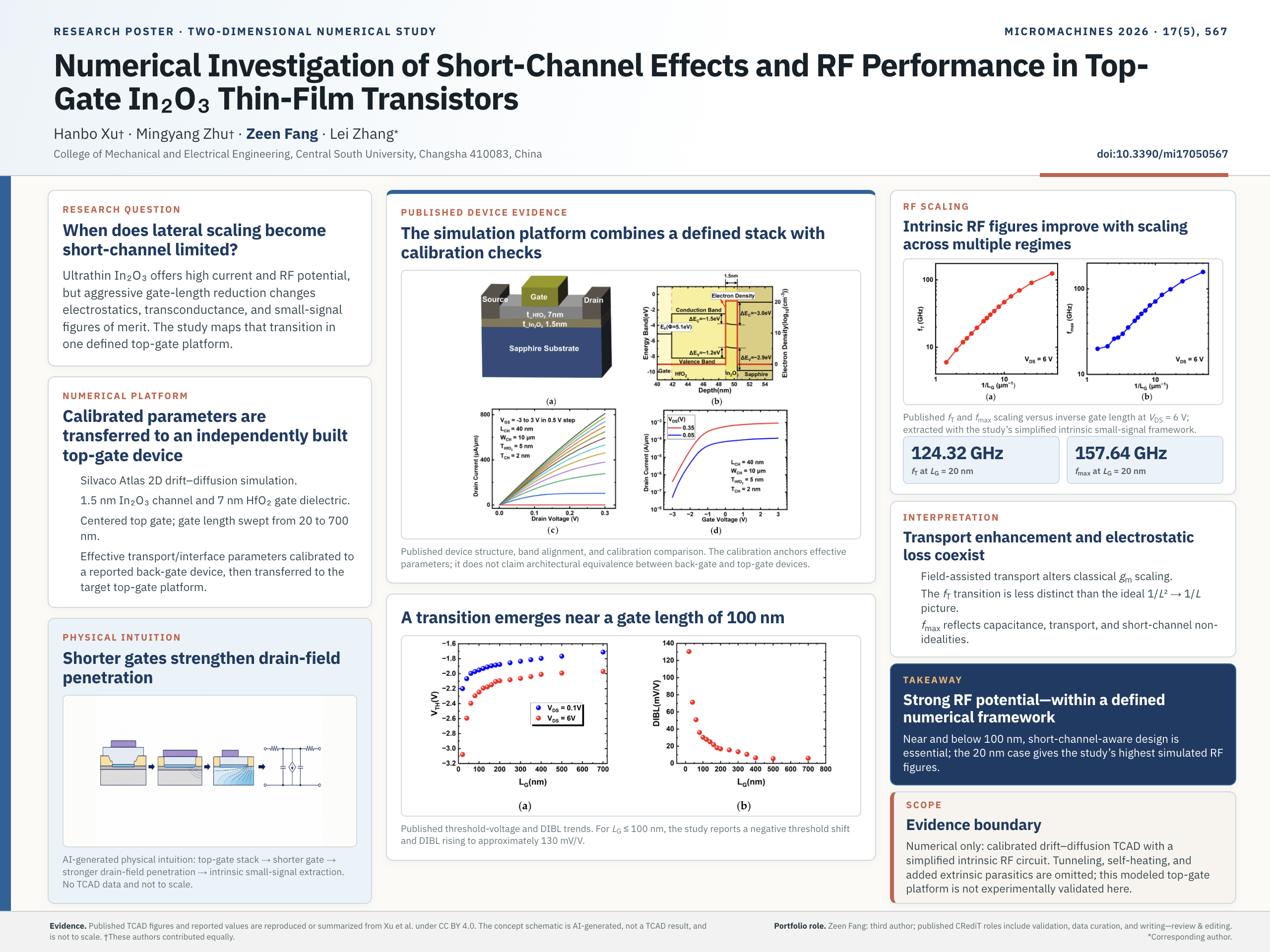
Reported transition region
Numerical long-channel to short-channel transition in gate length.
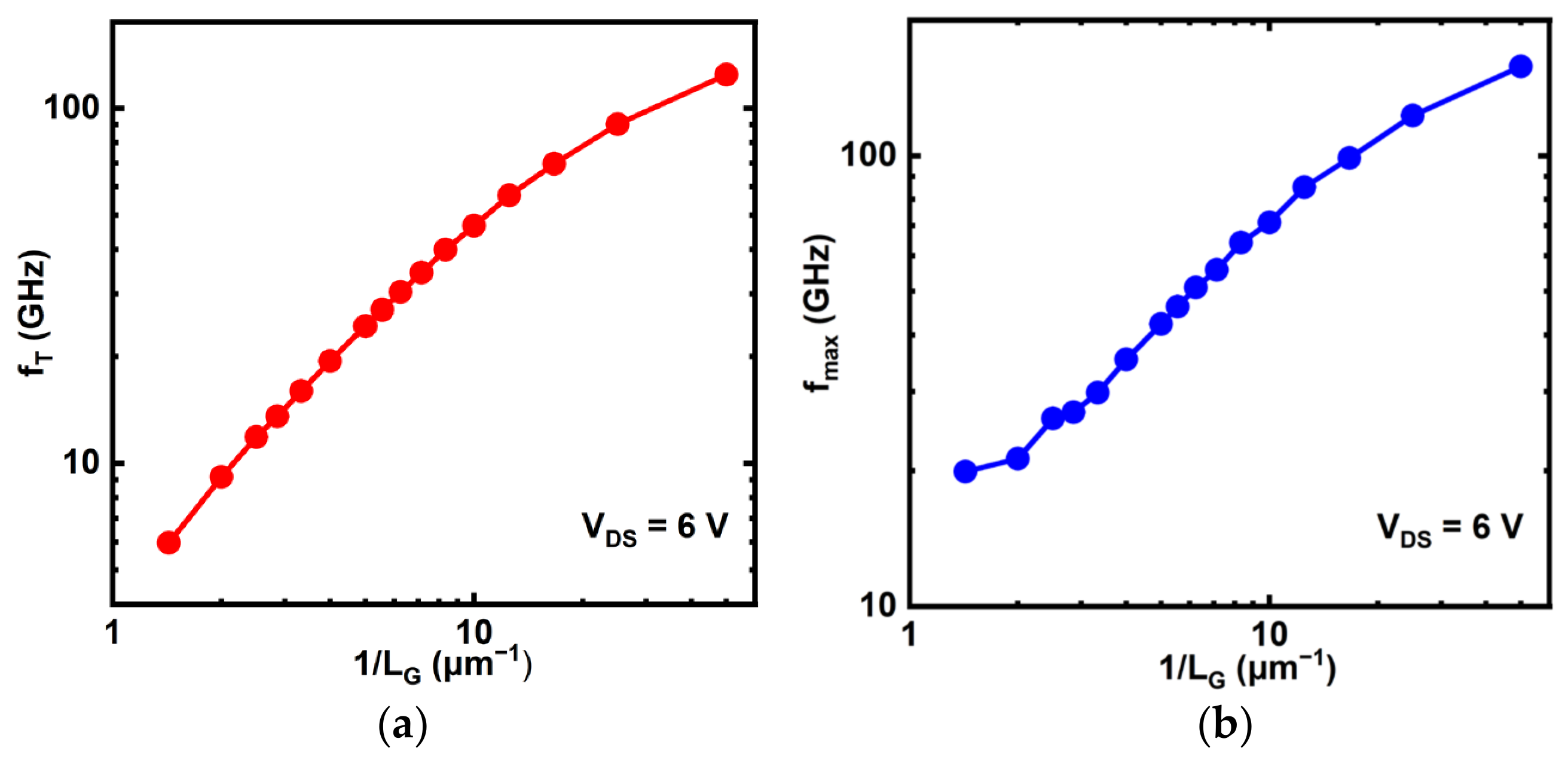
Simulated fT at 20 nm
Extracted from the study's simplified small-signal framework.
Simulated fmax at 20 nm
A numerical result, not a fabricated-device measurement.
Problem
Ultrathin In2O3 is promising for high-current and high-frequency electronics, but aggressive lateral scaling makes short-channel behavior increasingly important. A systematic view was needed of how gate length changes threshold behavior, transconductance, and RF figures of merit in a top-gate device architecture.
Approach
The paper uses two-dimensional Silvaco Atlas simulation for a top-gate In2O3 TFT with a 1.5 nm channel and 7 nm HfO2 dielectric across gate lengths from 20 to 700 nm. Effective material and interface parameters are calibrated against a previously reported back-gate experimental device, then transferred to the independently constructed top-gate simulation platform.
The numerical analysis connects DC characteristics, DIBL, transconductance, lateral electric field, field-dependent mobility, and a simplified small-signal RF equivalent circuit.
Reported results
The study identifies a numerical transition near a 100 nm gate length. For gate lengths at or below 100 nm, it reports a negative threshold-voltage shift and DIBL rising to approximately 130 mV/V, together with non-classical transconductance scaling linked to a crossover between field-assisted transport and gate-controlled channel modulation.
At 20 nm gate length, the simulation reports fT = 124.32 GHz and fmax = 157.64 GHz. The paper also reports a less distinct transition in fT scaling than classical long-channel expectations and multiple fmax scaling regimes shaped by capacitance, transport enhancement, and short-channel non-idealities.
Scope and next steps
The highlighted trends are study-level numerical results; the modeled top-gate platform is not experimentally validated here. Tunneling, self-heating, substrate effects, and additional extrinsic parasitics remain outside the current drift-diffusion and simplified intrinsic RF framework.