I am a B.Eng. candidate in Microelectronics Science and Engineering at Central South University, with an expected graduation date of June 2027. My current work lies at the device-circuit interface, spanning semiconductor-device simulation, memristor behavioral and circuit modeling, and the translation of device dynamics into circuit-level operating constraints.
I am seeking PhD opportunities for Fall 2027 to extend this foundation toward energy-efficient, low-jitter clock generation for high-speed SerDes. I hope to develop transistor-level analogue and mixed-signal design skills through focused circuit projects. Oscillator supply sensitivity offers a concrete starting point: understanding how physical coupling affects clock quality, then evaluating whether a targeted circuit change or limited calibration improves the jitter–power trade-off.
First authorModeling, simulation, analysis, and writing
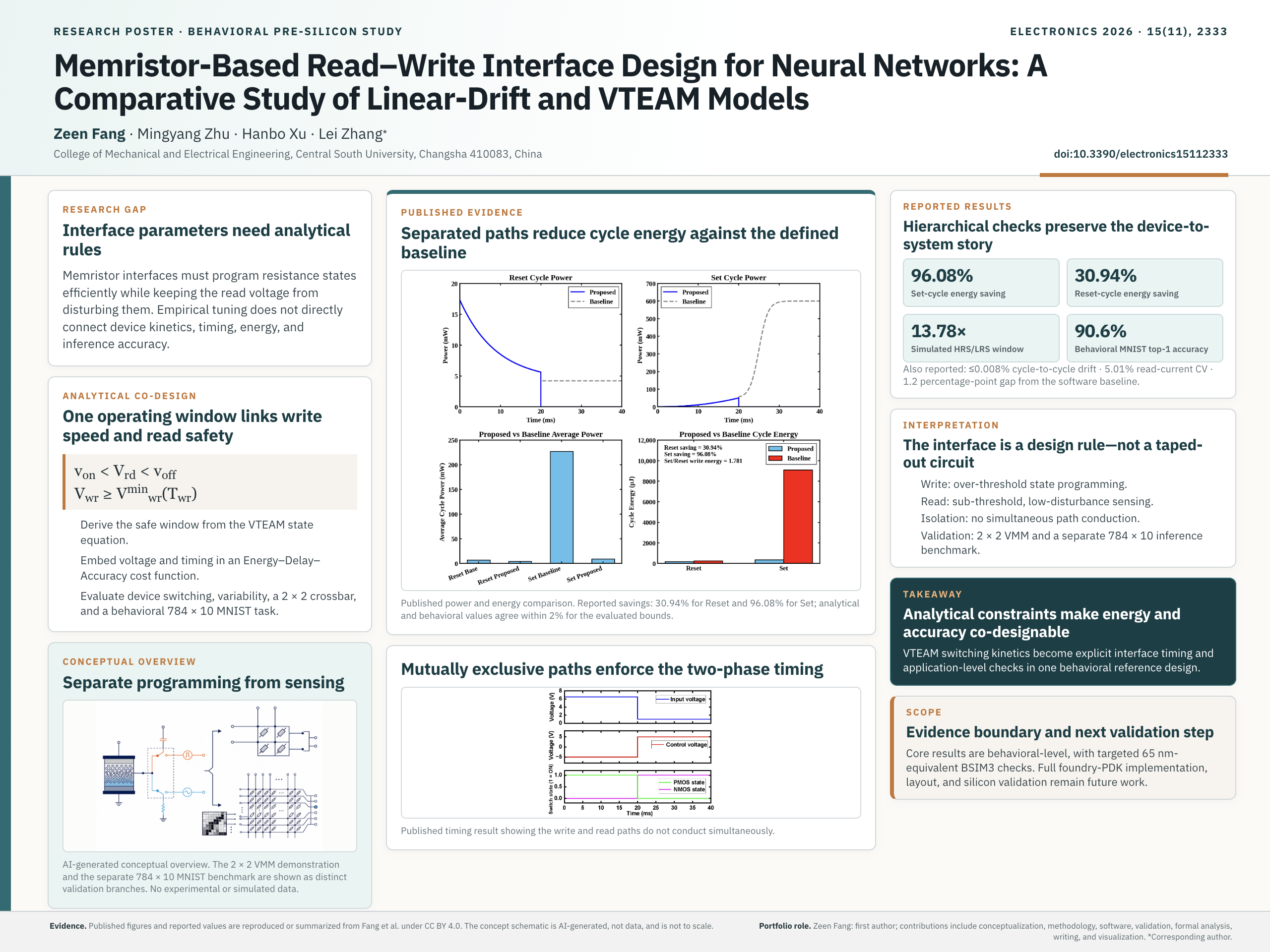
A behavioral-level, pre-silicon study deriving analytical read-write constraints from the VTEAM state equation and evaluating them from device to neural-network scale.
The published study reports a 13.78x resistance window and 90.6% MNIST top-1 accuracy, with 96.08% Set-cycle energy reduction against its defined behavioral baseline.
Third authorValidation, data curation, and manuscript review
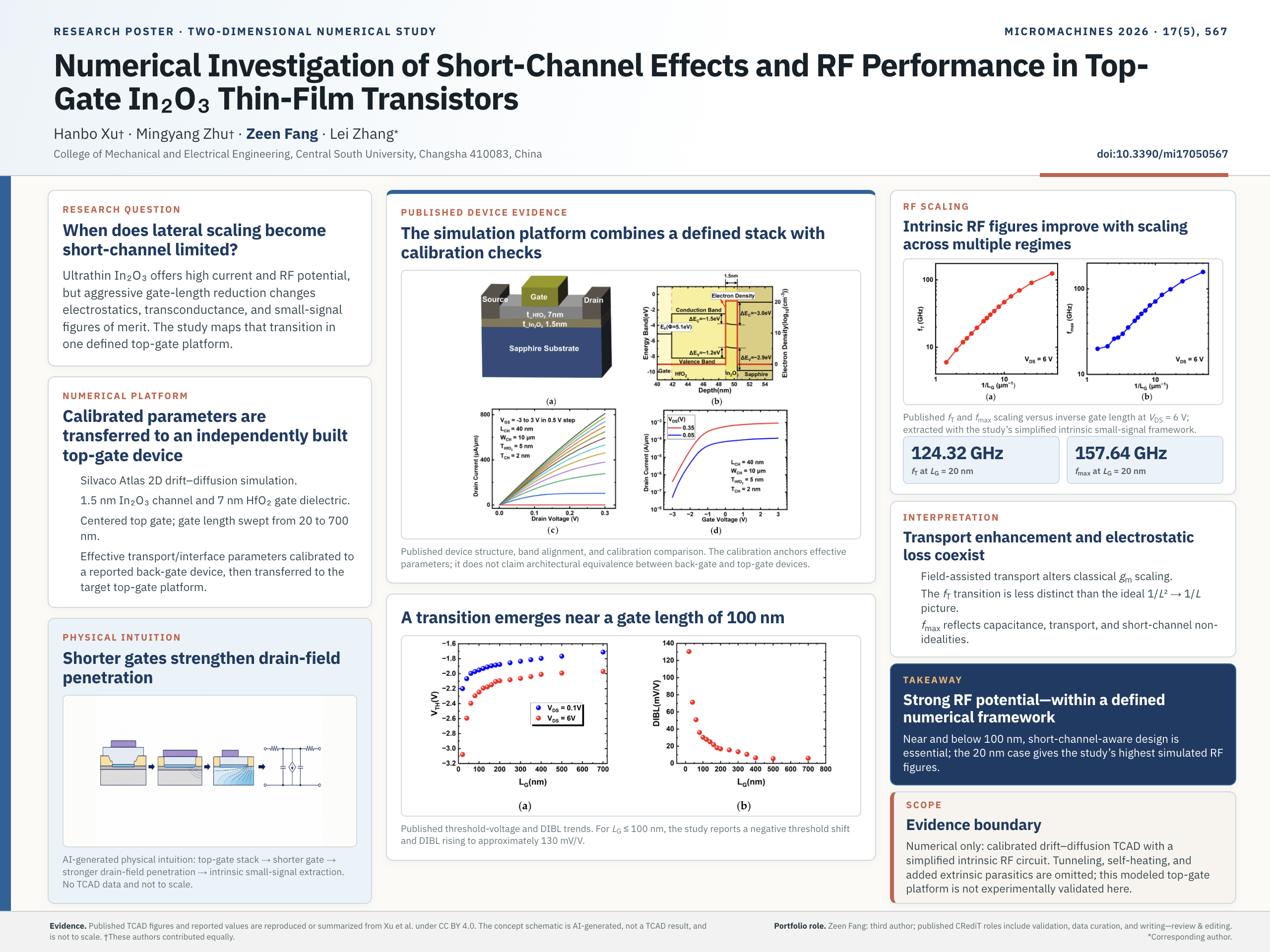
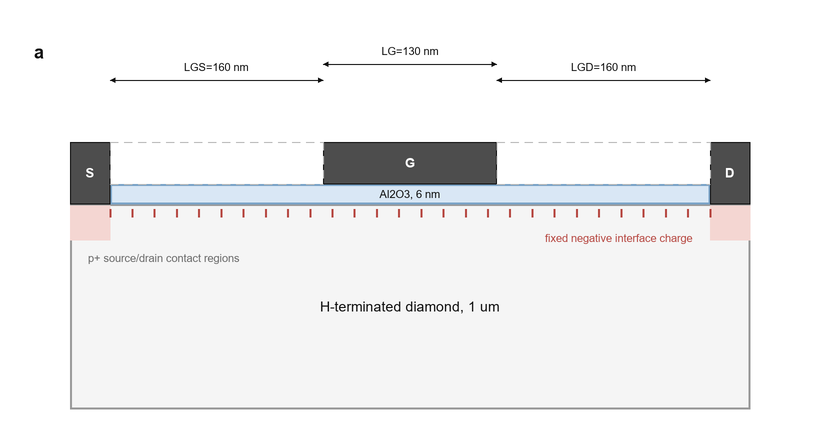
A two-dimensional numerical study of short-channel behavior and simulated DC/RF scaling across 20-700 nm top-gate In₂O₃ TFTs.
My credited roles were validation, data curation, and manuscript review and editing; the highlighted device and RF values are study-level numerical results.
Published work is listed above. Ongoing research and team engineering projects are identified here with their current evidence and status.
A Second-Order Memristor SPICE Model for Neuromorphic Circuit Analysis
Ongoing research · Manuscript in preparation · IEEE TCAS-I target · 2026-present
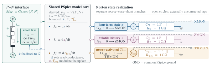
I am developing a PSpice second-order memristor model that separates a retained conductance state from a relaxing history state, with a power-activated auxiliary state. Matched-x paired-pulse, selected 1T1R, STDP-like, and compact 2 × 2 simulations connect internal-state attribution to circuit-level behavior.
Simulation-only: 11.16% matched-x interval sensitivity versus 1.01% for the separately simulated history-off family; STDP-like ΔG = -1.82% to +1.09%; 24 compact-array read cases with no more than 0.450% unit-range state disturbance. The target denotes planned submission style only.
Current PSpice implementation · simulation only
Team LDO competition project — Zengyi Huichuang Cup
10th National College Student IC Innovation and Entrepreneurship Competition · 2026
Team project
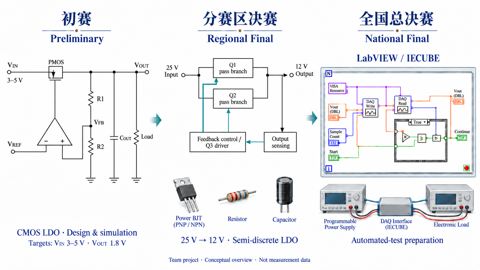
As a team member, I contributed to selected tasks across the competition stages: a 1.8 V CMOS LDO, eight simulation benches, a physical-verification trail, regional semi-discrete hardware, and national-stage automated-test preparation.
AI-generated conceptual overview, not the team's implementation schematic or measurement data. The LabVIEW interface illustrates national-final test preparation, not a completed or executable test system.
Selected team contributions under instructor guidance. CMOS work covers design and simulation; regional hardware is a separate semi-discrete LDO; automated testing remained preparation.
Design stages & original technical evidence
01
Team design & simulation
1.8 V CMOS LDO
SMIC 180 nm transistor-level work covering a PMOS pass device, bandgap reference, folded-cascode error-amplifier path, feedback, bias, and compensation, followed by eight dedicated simulation benches.
02
Physical workflow
Layout-level evaluation
Top-level layout integration, Calibre DRC/LVS/PEX, and post-layout simulation. The detailed case file keeps the unresolved DRC results and line-regulation gap visible.
03
Team hardware task
Regional-final LDO
BJT characterization and selection using TIP42C/TIP32C and BD139/BD135 candidates, followed by a 25 V-to-12 V semi-discrete LDO and regulation, stability, transient, and thermal evaluation.
04
Preparation only
Automated test workflow
IECUBE-3100/3839 and LabVIEW preparation for PWS/DIO/DMM control, voltage-accuracy, line/load-regulation and dropout scans, data logging, and result logic.
I constrained a Codex harness around local Silvaco ATLAS to turn paper reading, parameterized device sweeps, log parsing, figure generation, and scientific stop rules into one traceable research-training loop.
Codex supported workspace inspection, experiment matrices, parsing, and audits; ATLAS remained the solver, while I owned the physical assumptions, run authorization, stopping rules, and claim promotion.
My intended PhD direction is energy-efficient, low-jitter clock generation for high-speed SerDes. I am particularly interested in PLLs, supply-resilient oscillators and the analogue/mixed-signal circuits that determine clock quality. The following interests connect circuit-level noise mechanisms with link-level timing requirements.
Clock generation
Low-jitter PLLs & frequency synthesis
I am interested in how oscillator noise, phase-error extraction and loop bandwidth shape the jitter–power trade-off, including spur behaviour in fractional-N PLLs. I want to connect these block-level mechanisms with circuit improvements whose benefit remains meaningful after their power costs are included.
Integrated jitter · phase noise · spurs · total power
Circuit-level entry
Supply-resilient LC oscillators
I would like to study how tuning-bank parasitics and out-of-phase harmonic mixing turn supply disturbances into frequency and phase error. A particular interest is where passive filtering and cancellation remain effective across disturbance frequency, tuning codes and operating conditions, without sacrificing phase noise or power efficiency.
I want to relate PLL output jitter and noise in the clock path to the sampling-time budget of a selected high-speed serial link. My initial scope would be a clock source or supporting analogue/mixed-signal block, using link-level models to assess timing margin rather than assuming a complete transceiver design.
Timing margin · clock-path jitter · clocking power
First study: oscillator supply response. I would begin by reproducing a published LC-oscillator baseline, separating the tuning-bank and harmonic-mixing contributions, and examining the frequency-dependent limits of passive cancellation. A targeted circuit change or limited calibration would follow only if the baseline reveals a specific limitation; I would compare fixed and calibrated solutions under the same supply disturbances, process, voltage and temperature conditions, including parasitics and calibration overhead. Reproduction is preparation, not a research contribution on its own.
Research preparation · evidence from prior work
My published first-author memristor study trained me to derive operating constraints, test model predictions and carry a study through revision and publication. My ongoing second-order memristor work continues that training. I use AI-assisted workflows to automate repetitive simulations, connect software tools and organise data, with Git-based traceability and independent checks. Together with my mathematical preparation and initial team-based analogue-IC experience, these practices provide a foundation for learning transistor-level design through focused projects.
Device-to-specification translationPublished In₂O₃ numerical studyInterpreting device assumptions, scaling behavior, capacitance, and parasitic trends as circuit-design constraints.
IC workflow exposureTeam LDO competition projectSelected team tasks spanning schematic analysis, physical verification, post-layout evaluation, and semi-discrete hardware testing.
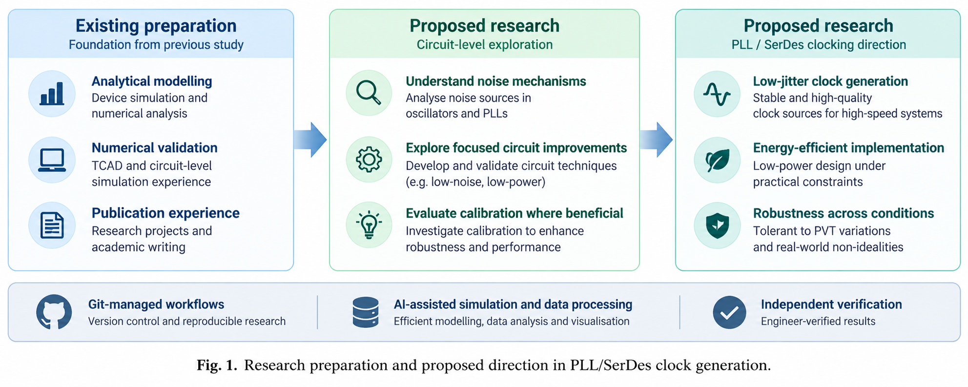
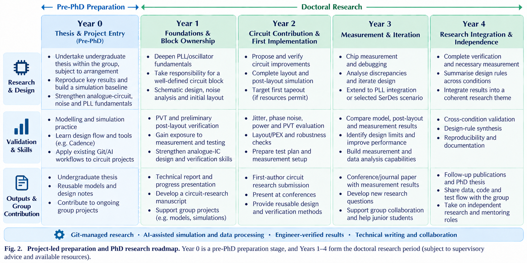
Research preparation & proposed directionExisting preparation and proposed research. Open the figure for a closer view.Proposed research development · Year 0–4
Year 0
Project-led preparation
Use undergraduate thesis work and a focused preparatory project to strengthen analogue-circuit and PLL fundamentals, reproduce a representative result and work towards a small circuit block.
Year 1
Foundations & block ownership
Deepen analogue and mixed-signal fundamentals through coursework and project work. Take responsibility for a well-defined block and connect models with transistor-level results.
Year 2
Circuit contribution & implementation
Develop and verify a focused improvement, assessing its jitter benefit and implementation costs. Work towards a first-author submission and an initial tapeout when readiness and resources permit.
Year 3
Measurement & iteration
Where resources permit, compare measurement with model and post-layout predictions. Use discrepancies to guide design iteration and develop experimentally supported findings.
Year 4
Research integration & thesis
Consolidate connected contributions into follow-up papers and a doctoral thesis. Share reusable simulation and testing workflows and contribute to collaborative projects.
View the full research roadmapVerification milestones
Progressive verification path
Proposed and resource-dependent
01Baseline gate
Reproduce a representative baseline and identify a specific performance limitation through consistent simulation and mechanism analysis.
Advance through transistor-level design, layout, DRC/LVS/PEX and post-layout verification, then assess the selected block's effect on PLL clock performance.
04Hardware gate
Proceed to prototype, tapeout, or measurement only when resources and earlier evidence permit.
These are candidate entry points, not completed designs or a thesis solution fixed in advance. I expect to begin with one well-grounded oscillator or PLL baseline, selected after reproduction and assessment of available project, fabrication, and measurement resources.
Education & Preparation
Central South University
2023.09-2027.06 (expected)
B.Eng. Candidate in Microelectronics Science and Engineering
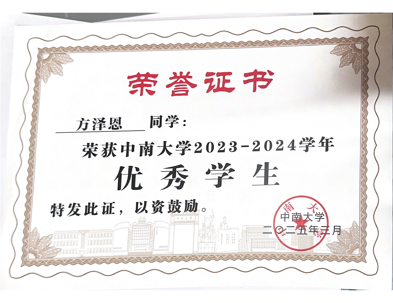
Outstanding Student · Central South University, 2023–2024
Selected coursework: Semiconductor Device Physics, Circuit Theory, Analog and Digital Electronic Technology, Signals and Systems, and Large-Scale Integrated Circuit Design.
Modeling & simulation
Semiconductor-device simulation, behavioral circuit modeling, MATLAB, and PSpice.
Full honours list · competitions, scholarships & student awards
Second Prize, National Final; First Prize, Central China Regional Final — 10th National College Student IC Innovation and Entrepreneurship Competition, Zengyi Huichuang Track · team award
Second Prize, Hunan Division; Excellence Award, National Final — 28th China Robot and Artificial Intelligence Competition, Humanoid Sprint · team awards
Honorable Mention, Mathematical Contest in Modeling · team award
Outstanding Student, College of Mechanical and Electrical Engineering, Central South University · certificate issued March 2026
Third Prize, Central South University Mathematics Competition · Non-Mathematics Category
First Prize, Hunan Division, 16th Chinese Mathematics Competition for College Students · Non-Mathematics Category A
First Prize, 8th Hunan Provincial College Students Mathematics Competition · Non-Mathematics Category A
Excellent Student Award, Highpower International Scholarship
Outstanding Student, Central South University
Second-Class Academic-Year Scholarship, Central South University
Fall 2027 PhD applications
Open to doctoral research conversations.
I am preparing applications to PhD programs in microelectronics, electrical and computer engineering, and related fields. If my device-to-circuit background aligns with your group's research, I would be glad to discuss potential doctoral directions.