First-author research / Published 2026
Memristor-Based Read-Write Interface Design for Neural Networks
A first-author, behavioral-level pre-silicon study connecting VTEAM design rules, read-write separation, energy analysis, and neural-network evaluation.
Academic poster

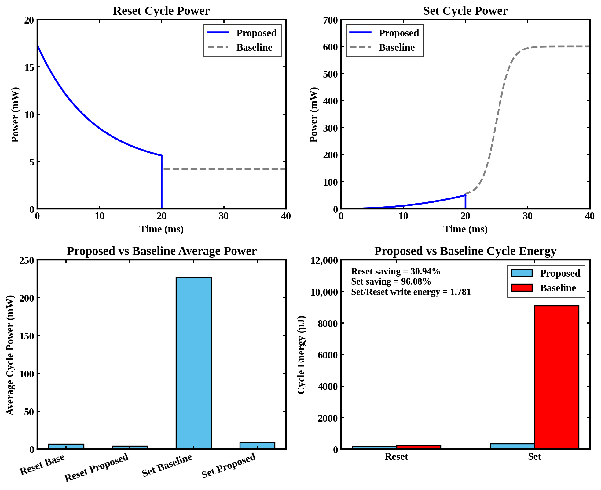
Set-cycle energy reduction
Reported against the defined no-separation behavioral baseline.
Resistance window
Simulated HRS/LRS ratio: 8681.68 / 630.02 ohm.
MNIST top-1 accuracy
Behavioral 784 x 10 evaluation; 1.2 points below software baseline.
Problem
Memristor interfaces must write resistance states efficiently while keeping read voltage from disturbing those states. Existing studies often tune these operating conditions empirically, leaving circuit designers without a compact rule that connects device kinetics, interface timing, energy, and application-level accuracy.
Approach
The study derives a closed-form safe operating window from the VTEAM state equation, then embeds the result in an Energy-Delay-Accuracy cost function. A two-phase over-threshold-write and sub-threshold-read strategy is paired with mutually exclusive PMOS/NMOS paths to separate programming and sensing.
The resulting parameter set is evaluated hierarchically in behavioral simulation: single-device switching, Monte Carlo variability, a 2 x 2 analog crossbar, and a separate 784 x 10 MNIST-style benchmark. Selected interface behaviors also receive targeted 65 nm-equivalent BSIM3 checks.
Reported results
Against the paper's explicitly defined no-separation baseline, the proposed timing strategy reports 30.94% Reset-cycle and 96.08% Set-cycle energy savings. It produces a simulated 13.78x resistance window, at most 0.008% cycle-to-cycle drift, and a 5.01% read-current coefficient of variation under the reported variability setup.
At the system level, the behavioral crossbar evaluation reports 90.6% MNIST top-1 accuracy, 1.2 percentage points below the software baseline. The paper reports agreement between the analytical predictions and behavioral results within 2% for the evaluated bounds.
Scope and next steps
Core results are behavioral-level, supplemented by targeted 65 nm-equivalent BSIM3 checks. Full foundry-PDK implementation, layout-aware simulation, peripheral-overhead accounting, and silicon validation are not established here.